TLC, QLC, MLC, SLC: which type of drive memory is better?

We independently test the products and technologies that we recommend.

We suggest studying the pros and cons of NAND, as well as choosing the optimal SSD from the general catalog, using filters by memory type.
What is NAND memory?
NAND is a type of non-volatile flash memory that is widely used in various data storage devices (SSD, USB flash drives, memory cards for smartphones, cameras). Initially, it contained one bit of information, but the desire to increase storage volumes while maintaining the dimensions of the device led to the natural development of technologies in this area. Over the past 10 years, several generations of multi-bit memory have emerged, making it possible to compress data and make storage accessible to all users. Manufacturers are also working towards reducing the size of the transistor. Initially, each cell occupied about 90 nm, and the current figure does not exceed 20 nm. The main problem with NAND remains its limited service life, which is calculated by the number of cell rewrite cycles. Durability depends on the intensity of use, but even budget drives can work for years without failure.


Differences and scope of application of TLC, QLC, MLC, SLC
Without going into complex technical details, memory types differ in basic characteristics - capacity, speed, service life and cost.
Many are mistaken in considering the QLC generation to be the most advanced. Each type has its own advantages and disadvantages that make NAND suitable for certain tasks. For convenience, let's compare the basic characteristics of all types:
| SLC (1st generation, 1 bit per cell) | MLC (2nd generation, 2 bits per cell) | TLC (3rd generation, 3 bits per cell) | QLC (4th generation, 4 bits per cell) | PLC (in development, 5 bits per cell) | |
|---|---|---|---|---|---|
| Capacity | small | average | big | big | very big |
| Performance | very high | high | average | low | low |
| Life time | very tall | average | average | short | short |
| Price | very high | average | average | low | minimum |
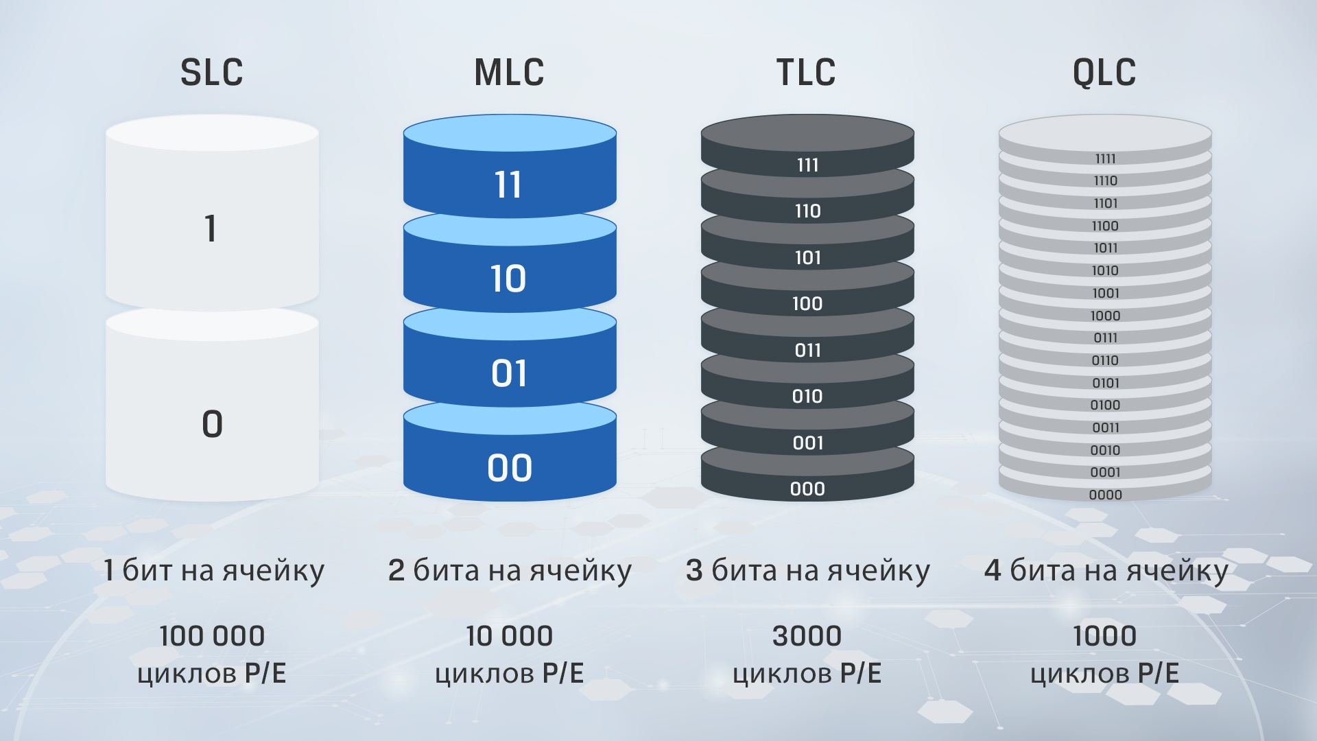
SLC (Single Level Cell, single-level) - memory that holds only 1 bit of data. Thus, if you place 10 corresponding transistors in a certain area, you can store only 10 bits of information. SLC is a very expensive and most efficient memory, which is used in military, scientific, and industrial fields where high performance and fault tolerance are required. It allows you to rewrite each cell 100,000 times and guarantees fast access to each of them, regardless of the load.
MLC(Multi Level Cell, multi-level) made it possible to double the storage capacity and store 2 bits of data in each transistor. Despite the more complex design, the devices have become cheaper, but the speed of access to information has also dropped slightly, as has the time between failures (10,000 cycles). The name still causes debate, since it would be more logical to use the abbreviation DLC (Dual Level Cell). It has gained popularity among servers and among enthusiasts due to its good balance between performance/reliability/price.
TLC(Triple Level Cell) is the most popular NAND memory in 2024 and will likely remain so for the next couple of years. Contains 3 bits of data in one transistor. It provides an optimal price/quality balance. It is worth noting that there is an informal division of TLC drives into consumer and corporate. The latter are of higher quality and equipped with advanced optimization technologies. For gaming PCs and servers, durability and performance are more important, so enterprise TLC wins here. Data read speed (when connected via PCIe) can exceed 7000 MB/s, and write speed - 6000 MB/s. The reliability of devices with such memory is not the highest, but usually manufacturers provide a warranty of 3–5 years, and the actual service life is much longer even if 50–100 GB of information is rewritten daily. Consumer TLCs are more modest and affordable. They have write and read speeds of about 2000 MB/s, which is more than enough for most tasks for many years. But high speed is maintained only when processing small amounts of data, and then there is a significant decrease. It is worth noting that durability largely depends on the total volume of the drive (more is better) and the intensity of use (less is better). Maximum service life is 3000 rewrite cycles.
QLC(Quad Level Cell, four-level) - memory capable of storing 4 bits of data in each cell. On the one hand, this implementation made it possible to increase the capacity of drives by 50% (compared to TLC), but a negative factor was regression in terms of performance and service life (1000 cycles). For this reason, QLC NAND is positioned as an effective and inexpensive replacement for the legacy hard disk drive (HDD). The devices are aimed at home use in PCs and laptops without long-term loads on the SSD, since after processing several gigabytes of data the speed decreases critically.


How is 3D NAND better than 2D NAND?
The development of multi-level cells at a certain point reached its limit for technical reasons:
- Firstly, further reduction of transistors (less than 15 nm) would lead to charge leakage and negative impact on adjacent memory slots.
- Secondly, the two-dimensional linear arrangement is limited by dimensions, because no one wants to carry around a flash drive or 1 TB drive the size of a brick.
Therefore, manufacturers began to look for ways to upgrade the planar 2D NAND structure. The first solution in the form of a three-dimensional array was presented by Samsung back in 2013. The new 3D NAND layout made it possible to increase memory cells not only in length and width, but also in height.
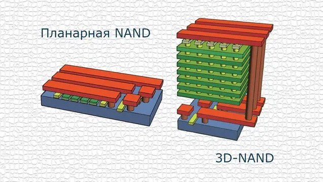
At the same time, a new approach to charge control was developed - the floating gate was replaced with an electronic trap. Updated data access algorithms have significantly improved the performance and service life of modern drives. It is worth noting that global memory manufacturers use their own approaches and structures to implement 3D NAND. Samsung's development was called V-NAND, while Toshiba and SanDisk chose BiCS (Bit Cost Scalable). Micron and Hynix decided not to stand out, so they use a standard name. Today, the 3D NAND structure has about 300 layers of transistors, which makes it possible to place terabytes of data in compact matrices. At the same time, the energy efficiency of the drives has increased, and the heating of the components has decreased significantly.


Prospects for further development of flash memory
As we have already found out, it makes no sense to experiment with the technical process of transistors, since this will lead to increased production defects and a decrease in the reliability of the storage. Therefore, companies are betting on progress in increasing capacity and optimizing data access algorithms.
Development of PLC 3D NAND (Penta Level Cell, five-level) is already underway, which in theory will allow placing 5 bits in each cell. However, practical implementation of QLC shows that this approach will not be cost-effective if the problem of performance degradation is not addressed. To be clear, in a single-level SLC the controller supplies a specific voltage to the cell and immediately gains access to the data. In the case of QLC, it will be necessary to provide one of 15 voltage options, which significantly reduces the speed of memory access. And for PLC the figure increases to 31, which leads not only to delays, but also to increased wear of transistors.
Manufacturers have already managed to solve many flash memory performance problems using technology. A good example is the NVMe communication protocol, which has become almost a standard for SSDs. Equipping with DRAM buffer memory guarantees consistently high speed of writing large volumes of information and processor access to it directly, bypassing RAM. Although this approach is still expensive and is used more for business. And for consumers, an SLC cache has been developed, which uses free memory cells of drives for intermediate one-bit recording, which speeds up performance when processing small amounts of data.
One of the Chinese companies, Yingren Technology, recently announced a new controller with a RISC-V structure, which solves the problem of overheating and throttling. It will be consumer-oriented and stand out for its minimal cost. The maximum capacity of such SSDs will reach 8 TB.
In the spring of 2024, South Korea made a breakthrough in the development of the cell structure itself, introducing the world to phase change memory (PCM). The operating principle is based on changing the state of a substance - crystallized or amorphous. But the development requires solving problems with energy efficiency, since the conversion requires significant electricity consumption and is accompanied by heat generation. And the production process itself is quite expensive, so ordinary consumers should not hope for such innovations in the near future.


Articles, reviews, useful tips
All materials